-
 206-310-3624
-
 support@pcbinternational.com
206-310-3624
support@pcbinternational.com
What is the difference between Controlled Dielectric and Controlled Impedance regarding PCB fabrication? The purpose of controlling dielectric or impedance is essentially the same, to achieve a target impedance on one or more signal lines on a printed circuit board. For example, your design has a USB signal pair that must have an impedance of 90 ohms (±10%) to function properly. To make sure this will happen, there are many factors that need to be considered and calculated such as trace width, spacing between copper features on the same layer, distance between copper features on other layers, the Dk (dielectric constant) of the laminate used to manufacture the board, as well as a few other factors.
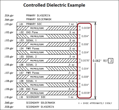
If you are comfortable with tackling the calculations yourself, you would opt for the Controlled Dielectric approach to control your own impedance. After making all the necessary calculations, you would need to provide us with your custom stack-up that specifies exactly what dielectric spacing is needed between your copper layers as well as layout your traces with the correct trace and space. On our instant PCB quote page, you would need to select CONTROLLED DIELECTRIC since we would not be recalculating the impedance for you, nor testing the board to ensure the impedance is met. We would print the copper features on your board as we see them in the Gerber and follow the dielectric thicknesses that you specify.
If you would prefer to have our engineers calculate the impedance for you, we would need to know which traces need to be controlled, what impedance is required and in reference to which copper layers.
Tip: The easiest way to specify which traces need to be controlled is to make these traces a unique trace width such as 6.5 mils. Even if you have hundreds of 6-mil wide signal lines on your board, we can easily search the Gerber for a specific width to find the 6.5-mil critical lines. If the impedance traces are the same width as many other traces, it will becomes challenging to determine which traces are to be controlled.
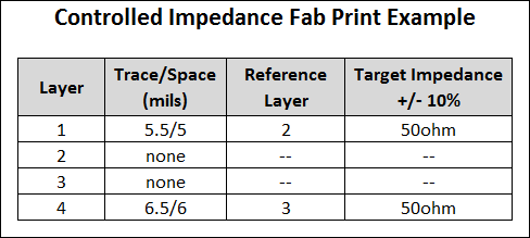
When placing an order for a printed circuit board with Controlled Impedance requirements from PCB International, we handle the brunt of the work. We perform the calculations for trace and space, use the correct dielectric spacing between your layers, and run a TDR test to confirm that the correct impedance is met. The stack-ups and impedance calculations will be provided to you upon request for your reference.
If you have any questions regarding controlled dielectric or impedance control for your PCB design, please contact us for assistance. The definitions for the topics discussed on this page are below.
Dielectric – The measure of resistance to the flow of electrical current, usually expressed as Dk (dielectric constant).
Dielectric can also mean an electrical insulator that can be polarized by an applied electric field. When a dielectric is placed in an electric field, electric charges do not flow through the material, as in a conductor, but only slightly shift from their average equilibrium positions causing dielectric polarization. Because of dielectric polarization, positive charges are displaced toward the field and negative charges shift in the opposite direction. This creates an internal electric field, which reduces the overall field within the dielectric itself.
To a PCB manufacturer, a controlled dielectric implies that specific thicknesses between layers are required.
Controlled Impedance - The matching of substrate material properties with trace dimensions and locations in an effort to create a specific electrical impedance for a signal moving along a trace. Controlled impedance implies that the PCB is manufactured so that the impedance of traces is within a certain percentage of a specified value.
Time Domain Reflectometry (TDR) - A measure of the reflections and spurious signals in a conductor arising from the source coupling into non-ideal impedances (e.g. the connecting wiring and termination). It is a common test used for high-speed digital and analog work.