-
 206-310-3624
-
 support@pcbinternational.com
206-310-3624
support@pcbinternational.com
High-density interconnect, or HDI, circuit boards are printed circuit boards with a higher wiring density per unit area than traditional printed circuit boards. In general, HDI PCBs are defined as PCBs with one or all of the following: microvias; blind and buried vias; built-up laminations and high signal performance considerations. Printed circuit board technology has been evolving with changing technology that calls for smaller and faster products. HDI boards are more compact and have smaller vias, pads, copper traces and spaces. As a result, HDIs have denser wiring resulting in lighter weight, more compact, lower layer count PCBs. Rather than using a few PCBs in a device, one HDI board can house the functionality of the previous boards used.
At PCB International, we strive to provide the best quality printed circuit boards with wide variety of design characteristics to suit all your project needs; we can supply printed circuit boards up to 36 layers, and copper weight up to 20oz. PCB International’ Instant Online Quote Engine can provide quotes for boards requiring copper weight up to 2oz, and up to 24 layers; printed circuit boards requiring copper weight of 3 - 20oz and/or layer count 25 – 36 layers require custom quoting. For HDI PCBs with blind and buried vias, custom quoting is required; you can do so by emailing your requirements and/or Gerber files to support@pcbinternational.com.
The primary benefit of HDI printed circuit boards is the capability to “do more with less”; with copper-etching technology continuously refined for better precision, it became possible to combine functionalities of multiple PCBs into one HDI PCB.
Shortening the distance between devices and trace spaces, HDI PCBs allow for deployment of a large number of transistors for better performance in electronics while lowering power consumption. Signal integrity is also improved due to the shorter distance connections and lower power requirements. Other performance improvements over conventional PCBs include stable voltage rail, minimal stubs, lower RFI/EMI, and closer ground planes and distributed capacitance.
Additionally, consider using a HDI printed circuit board for the following benefits:
A HDI PCB is usually found in complex electronic devices that demand excellent performance while conserving space. Applications include mobile /cellular phones, touch-screen devices, laptop computers, digital cameras, 4/5G network communications, and military applications such as avionics and smart munitions.
Automotive and aerospace industries, where lower weight can mean more efficient operation, have been utilizing HDI PCBs at an increasing rate. Like almost everything else, cars are becoming more connected and computerized. Today’s cars have around 50 microprocessors on board that play a role in engine controls, diagnostics, safety features and other conveniences. Many advanced features such as onboard WiFi and GPS, rearview cameras and backup sensors rely on HDI PCBs. As automotive technology continues to advance, HDI tech will likely play an increasingly important role.
HDI PCBs are also prominently featured in medical devices; advanced electronic medical devices such as equipment for monitoring, imaging, surgical procedures, laboratory analysis etc., incorporate HDI boards. The high-density technology promotes improved performance and smaller, more cost-effective devices, potentially improving the accuracy of monitoring and medical testing.
Industrial automation requires abundant computerization, and IoT devices are becoming more common in manufacturing, warehousing, and other industrial settings. Many of these advanced equipment employ HDI technology. Today, businesses use electronic tools to keep track of inventory and monitor equipment performance. Increasingly, machinery includes smart sensors that collect usage data and connect to the internet to communicate with other smart devices, as well as to relay information to management and help optimize operations.
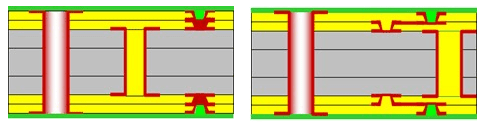
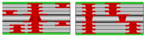
Depending on the design requirements, HDI Printed Circuit Boards can utilize different layering methods to achieve the desired performance.
PCB International strongly recommends sending us the Board Stackup to support@pcbinternational.com so we may confirm your desired HDI board design can be successfully manufactured.
HDI PCB (1+N+1): Simplest HDI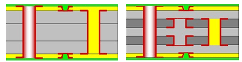
Further design guidelines/recommendations for High-Density Interconnect Printed Circuit Boards are available upon request; contact PCB International at support@pcbinternational.com or your Account Representative to inquire more!